
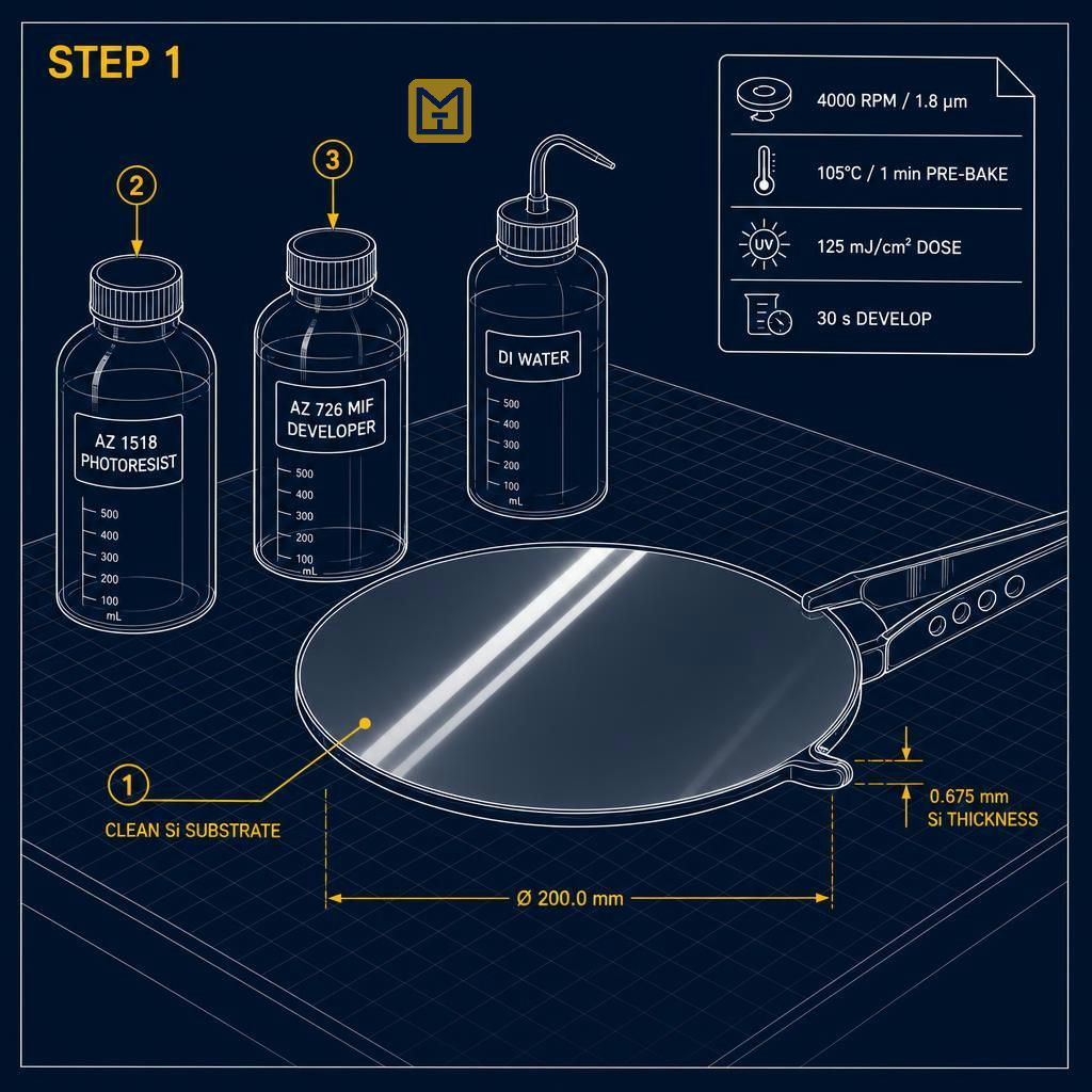
AZ 1518 Photoresist Process (TU Delft LSW Recipe)
by Nikos Papadopoulos
A step-by-step positive photolithography process using AZ 1518 photoresist to pattern a silicon substrate for wet etching, yielding a 1.8 µm resist layer. Written for cleanroom users reproducing the Kavli Nanolab Delft LSW recipe on an HBG_uMLA maskless aligner.
Silicon substrate
1 clean silicon wafer or chip (the substrate to be patterned)
HMDS
Hexamethyldisilazane adhesion promoter, applied by vapour deposition (improves resist adhesion)
AZ 1518 photoresist
Positive-tone photoresist, MicroChemicals GmbH, enough to cover the substrate (~1–3 ml)
AZ 726 MIF developer
Metal-ion-free TMAH developer, sufficient to immerse the substrate (develops exposed resist)
Deionised water
For stopping development and final rinse (stops and clears developer)
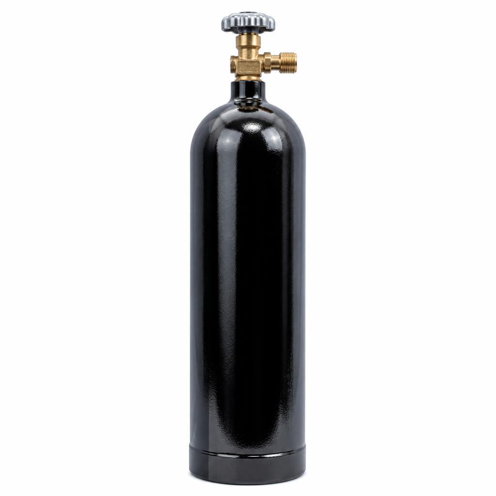
Nitrogen gas
Filtered dry N2 for blow-drying the substrate (dries surface after rinse)
Step 1 of 7
Recipe parameters and materials checklist
MATERIALS
TOOLS
Wafer tweezers
CHECK MATERIALS AND RECIPE
- ✓Confirm silicon wafer is clean
- ✓Verify all wet chemistry is fresh
- ✓Note all recipe parameters before starting
Instructions
• Tone: positive. Reference: AZ 1518 photoresist, MicroChemicals GmbH. • Target film: 1.8 µm at 4000 RPM (per spin curve). • Pre-bake: 1 min at 105 °C. Exposure: dose 40, focus +2, at 125 mJ/cm². • Development: 30 s in AZ 726 MIF; stop 30 s in water then rinse with water. • Confirm substrate is clean silicon and all wet chemistry is fresh before starting. • Gather all materials and tools listed above; verify expiry dates on AZ 1518 and AZ 726 MIF.
Time & Waiting
Active work
10 minutes
People
1 person
Swipe or use ← → keys
Want to follow this guide step by step or log your own build?
Open in the Makeit App